
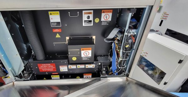
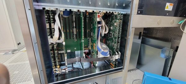
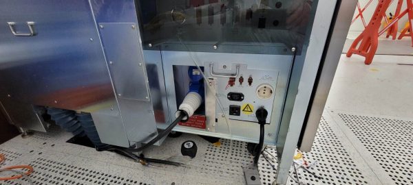
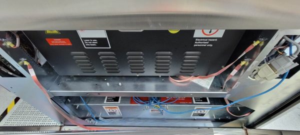


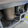
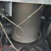
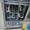
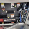


Description
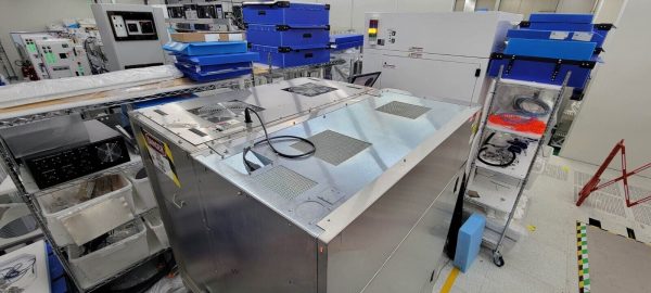
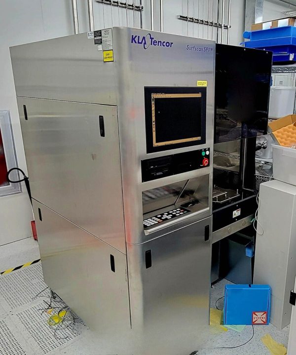
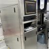
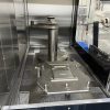
KLA-Tencor Surfscan SP1-TBI Unpatterned Wafer Defect Inspection Systems – Year 2001
KLA-Tencor Surfscan SP1-TBI Unpatterned Wafer Defect Inspection Systems :
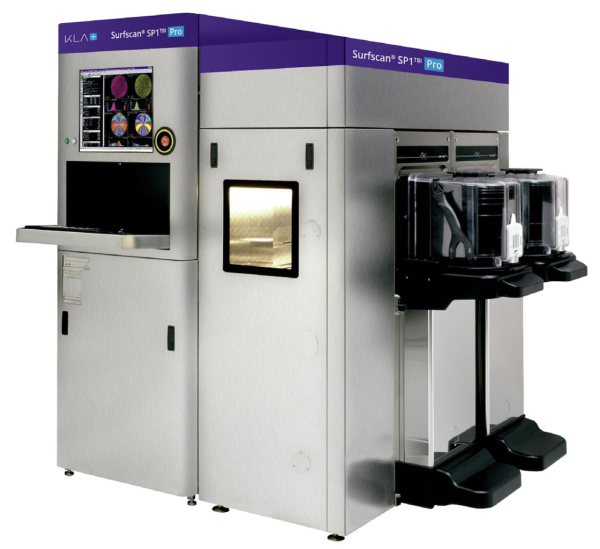
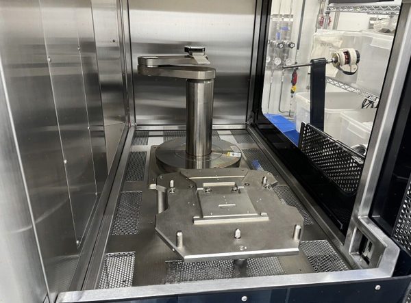
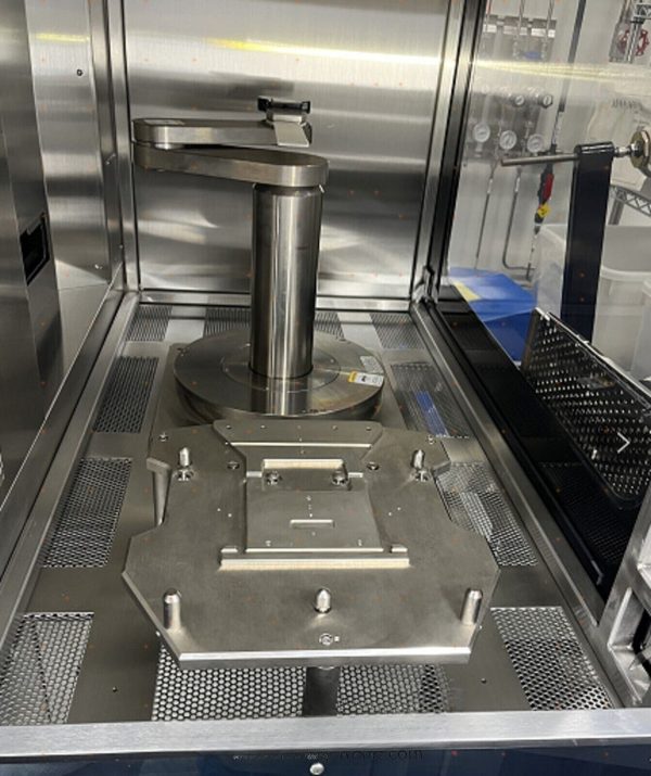
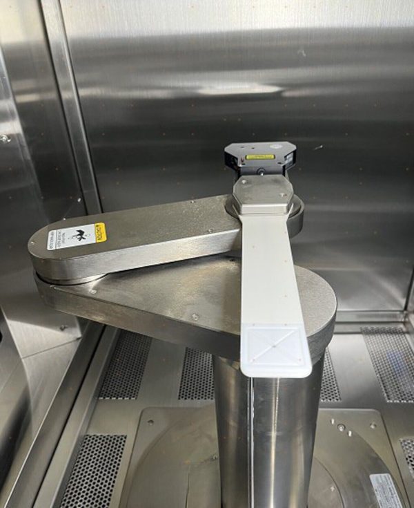
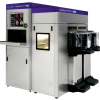
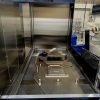
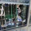
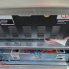
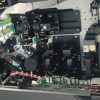
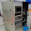
Surfscan® SP1TBI Pro / SP1DLS Pro Unpatterned Wafer Defect Inspection Systems
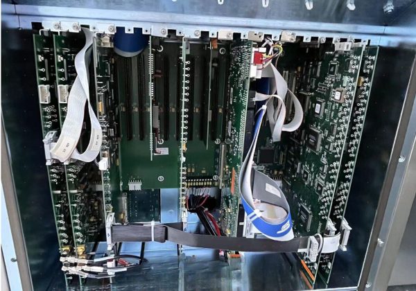
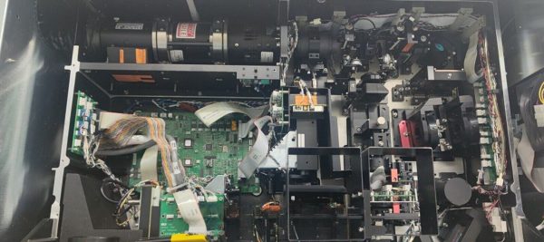
The Surfscan® SP1TBI Pro and SP1DLS Pro systems are industry-proven process control workhorse systems for unpatterned wafer inspection suited for emerging technologies such as RF, automotive, SiC, GaN, LED and more. The system facilitates the qualification and monitoring of processes and tools required by substrate, IC, equipment and materials manufacturers across the semiconductor ecosystem.
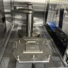
Built on the successful Surfscan® platform, the SP1TBI and SP1DLS Pro tools are designed to capture and classify critical defects in real-time on bare wafers, smooth & rough films and stacks, photoresists and litho stacks. By discovering and identifying critical defects and surface quality issues early on, the Surfscan SP1 Pro tools enable faster identification of process and tool issues, driving faster ramp, higher yield and improved profitability. High sensitivity mode provides defect detection down to 60nm on the SP1TBI and 50nm on the SP1DLS on prime bare silicon and high throughput mode options serve volume production. The SP1 Pro series tools satisfy R&D pathfinding applications and are equally suited to provide critical tool monitoring inspection points in a full manufacturing environment, all in a single tool.
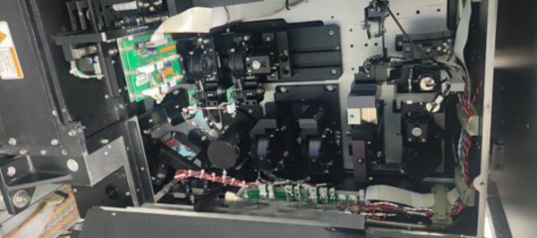
Triple Beam Illumination (TBI) provides a variety of methods for characterizing wafer quality
Dual Laser System (DLS) uses multiple lasers and detectors to combine brightfield, darkfield and nanotopography to capture a wide range of defects.
Silicon based tool qualifications and process monitoring for >50nm sensitivities in 150-300mm wafer formats
High sensitivity mode extends capabilities for R&D applications
Product manufacturing restarted for increased serviceability and predictability of supply
Standardized handler for flexible configurations
Defect Sensitivity
Productivity
▪ Oblique Illumination provides best sensitivity for particle detection on smooth surfaces and allows configurability for improving sensitivity on rough blanket films▪ Normal Illumination is ideal for detecting mechanical scratches for equipment monitoring or slip lines for epitaxial processes
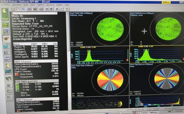
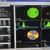
▪ Brightfield Differential Interference Contrast (BF-DIC) allows for improved capture of defects with surface height changes▪ Haze maps graphically represent full wafer surface conditions / quality
▪ Throughput can be increased with a licensed productivity option for faster time to results on 200mm
wafers (with vacuum handling)
▪ Solid State Laser provides longer life with less need for service (standard on DLS; option on TBI)▪ KLA Ecosystem compatibility with Klarity + eDR SEM review
▪ Full Factory Automation meets SEMI Standards
Device Manufacturers Choice for Automotive, RF, & μLE
Measure at critical process inspection points to monitor and control process tools
▪ Flexible optical configurations accommodates a wide range process conditions
▪ Adapter plate available to quickly convert between 150mm & 200mm wafer diameters
▪ Industry standard for wafer qualification – wafer manufacturer OQC and wafer fab IQC ▪ Capable of measuring 200mm substrates up to 1500μm thickness and up to 75μm warp ▪ Onboard grading capability with up to 4 x 200mm load port sorting stations
▪ Industry standard for process tool qualification
▪ Inspection can be optimized for Epi GaN-on-Si, AlN, and other exotic films ▪ High sensitivity mode extends capabilities for R&D